PCB Segmentation with SAM
SUMMARY
This section demonstrates how to use the Cornea module for PCB (Printed Circuit Board) segmentation in electronics manufacturing and inspection environments.
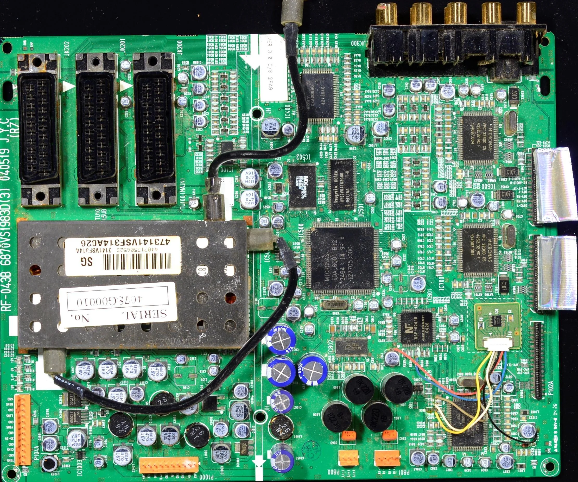
PCB segmentation is the task of identifying and isolating individual PCBs or regions of interest on a panel, even when they are densely packed, partially occluded, or contain complex patterns. Traditional methods often fail due to varying colors, silkscreen markings, and overlapping components.
segment_image_using_sam is used to robustly extract accurate masks for each PCB or region, enabling downstream inspection, pick-and-place, or quality control tasks.
Details on the skill, code, and practical usage are provided below.
The Skill
For electronics manufacturing, it is critical to accurately isolate each PCB or region of interest for inspection, pick-and-place, or defect detection.
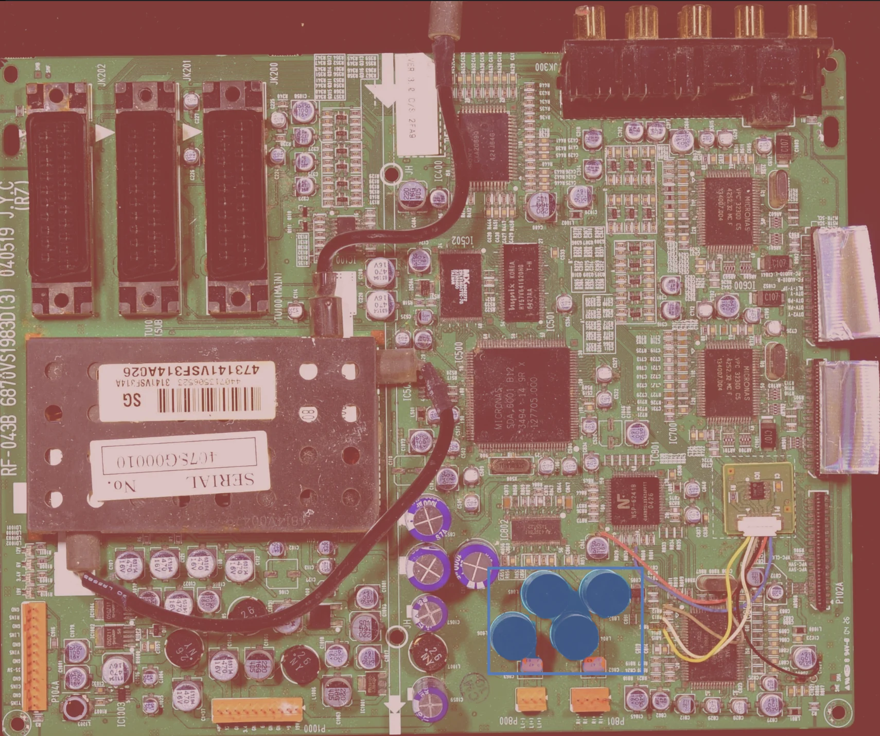
Bounding boxes alone are insufficient for complex layouts or when PCBs are closely packed. segment_image_using_sam provides pixel-accurate masks that define the exact extent of each PCB, even in the presence of silkscreen, solder, or overlapping components.
This segmentation mask enables industrial applications such as:
- Automated optical inspection (AOI)
- Pick-and-place targeting
- Defect and anomaly detection
- Quality control and traceability
See below for a code example demonstrating how to load a PCB panel image, segment the PCBs using SAM, and access the resulting annotations for further processing or visualization.
The Code
from telekinesis import cornea
from datatypes import io

# 1. Load a PCB panel image
image = io.load_image(filepath="pcb_panel.jpg")

# 2. Define bounding boxes for regions of interest
bounding_boxes = [[x_min, y_min, x_max, y_max], ...]

# 3. Segment objects using SAM
result = cornea.segment_image_using_sam(image=image, bbox=bounding_boxes)

# 4. Access COCO-style annotations for visualization and processing
annotations = result["annotation"].to_list()
This code demonstrates how to load a PCB panel image, segment the PCBs using segment_image_using_sam, and access the resulting masks and bounding boxes for further processing or visualization.
Going Further: From Segmentation to Inspection
Once the PCBs are segmented, the following steps enable advanced inspection and automation:
- Region-of-interest extraction: Use the segmentation mask to crop or focus on individual PCBs for detailed analysis.
- Defect detection: Apply inspection algorithms to each segmented region to identify missing components, solder defects, or anomalies.
- Pick-and-place guidance: Use the mask to determine safe pick points for robotic handling.
- Traceability: Assign unique IDs to each PCB for tracking through the manufacturing process.
Key Takeaway
PCB segmentation transforms a visually complex panel into explicit, actionable regions for inspection, automation, and quality control.
Other Typical Applications
- Automated optical inspection (AOI)
- Pick-and-place
- Defect and anomaly detection
- Quality control and traceability
- Panelization and depanelization
- Component counting
Related Skills
segment_image_using_samsegment_using_rgbsegment_using_hsv
Running the Example
Runnable examples are available in the Telekinesis examples repository. Follow the README in that repository to set up the environment. Once set up, you can run a similar example with:
cd telekinesis-examples
python examples/cornea_examples.py --example segment_image_using_sam