

PCB Segmentation with SAM
SUMMARY
Isolate individual PCBs or regions of interest on a panel, even when they're densely packed or visually similar due to silkscreen markings and overlapping components. segment_image_using_sam returns a pixel-accurate mask per board or region, supporting automated optical inspection, pick-and-place targeting, and defect detection.
Raw Sensor Input
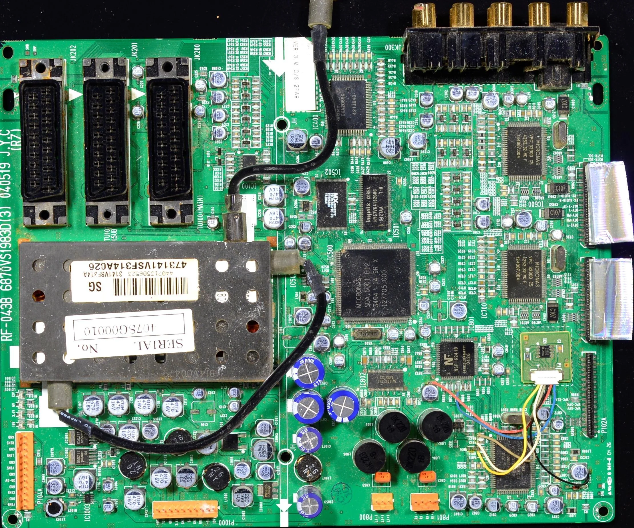
Raw sensor input showing a single PCB.
Segmentation and Masks
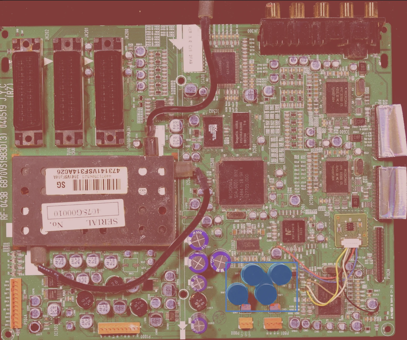
Segmented image showing masks and bounding box for components on the PCB.
Code
python
from telekinesis import cornea

# `image` is a datatypes.Image (or np.ndarray) of the PCB panel.
# `bboxes` is one [x1, y1, x2, y2] box per PCB or region of interest on
# the panel.
segmentation_results = cornea.segment_image_using_sam(
    image=image,
    bboxes=bboxes,
    mask_threshold=0.5,
)

# Each result carries a bounding box, a mask-quality score, and an
# encoded segmentation mask for that board — crop to the mask for
# per-board inspection, or use it to guide a pick-and-place robot.
for result in segmentation_results:
    box = result.bbox
    score = result.score
    mask = result.segmentation